I've always been fascinated with phased array antenna systems. In my opinion, they are one of the coolest and most intriguing RF technologies, powering things like radar and 5G systems. They work by combining an array of antennas in a way that directionality can be obtained through either constructive or destructive interference. In other words, phased arrays can essentially steer radio waves without any moving parts (a technique known as beamforming). To do this, the phase of each element of the array must be independently manipulated.
![]()
Note: In this article, I may use the terms "time difference unit" and "phase shifter" interchangeably. They are different, but very similar. What I describe in this article is technically a time difference unit as it uses lengths of transmission line to delay RF signals. It implements a transport delay, which is equivalent to a linear phase shift across all frequencies. However, for simplicity I will refer to phase shift and time delay in this article interchangeably, as their difference is minute.
For a while, I have been pondering how I could construct a phased array antenna with very low cost and complexity with the intention of using it for radio astronomy, moonbounce, satellite work, and more. My first idea was to use an array of antennas each feeding into its own SDR. The SDRs would need to be phase-coherent, meaning they would share a common clock source, allowing the phase difference of the different SDRs to be corrected by calibration. This means that a radio signal transmitted an equal distance away from each antenna would be received at the same time by every SDR. Using software, the system could generate relative phase shifts for each receiver, thus accomplishing my beamforming goals. This technique also allows the phase difference of an incoming signal along each of the receivers to be detected, allowing the signal's direction to be determined. This idea of using software to phase shift signals is powerful and has some distinct advantages, notably the phase-detection capabilites. However, the cost of using a radio transceiver for every element of the array is enormous. I considered modifying cheap RTL-SDRs for phase coherency, but that would only grant reception capability. Furthermore, each element of the array would require its own RF front end, consisting of LNAs, filters, and more. In short, large phased arrays would require a lot of redundant hardware, which can be very expensive.
My solution to this is to use a device directly after each antenna (from a receiving point of view) that would generate an arbitrary phase shift via commands from a microcontroller or single board computer. The microcontroller would compute the phase shifts from a function taking θ (the angle that the array is "pointing" at) as the input parameter. There would be this phase shifter or time delay unit after each antenna which feeds into a common RF front end and SDR transceiver. The phase shifter in this article was designed to minimize cost and allow production in mass quantities (for large phased arrays).
The Design
The overall goal of this device is to delay RF signals by a specified amount. The simplest way to do this is to force the signals to travel further. In HF antennas, this is commonly achieved by switching out different lengths of coax. The longer the transmission line, the larger the time difference. This is the method that I will be using in this design. However, since I want this phase shift circuit to work at microwave frequencies, it must be approached differently than an equivalent HF or VHF circuit. This design uses microstrip lines, which is method of creating transmission lines that are etched onto circuit boards. They work well at high frequencies and are cheap to produce. Instead of etching them into a PCB, I will use a plastic substrate with copper tape as the ground plane, and the microstrip lines cut from copper tape on the top layer. This is cheaper than ordering mass quantities of PCBs because the transmission line lengths required to produce the necessary time delay are relatively long, requiring large PCBs. Additionally, this is a good method for me because I have access to a Cricut machine capable of cutting the copper tape with precision. Below is a simple block diagram of the phase shifting circuit suitable for receiving:
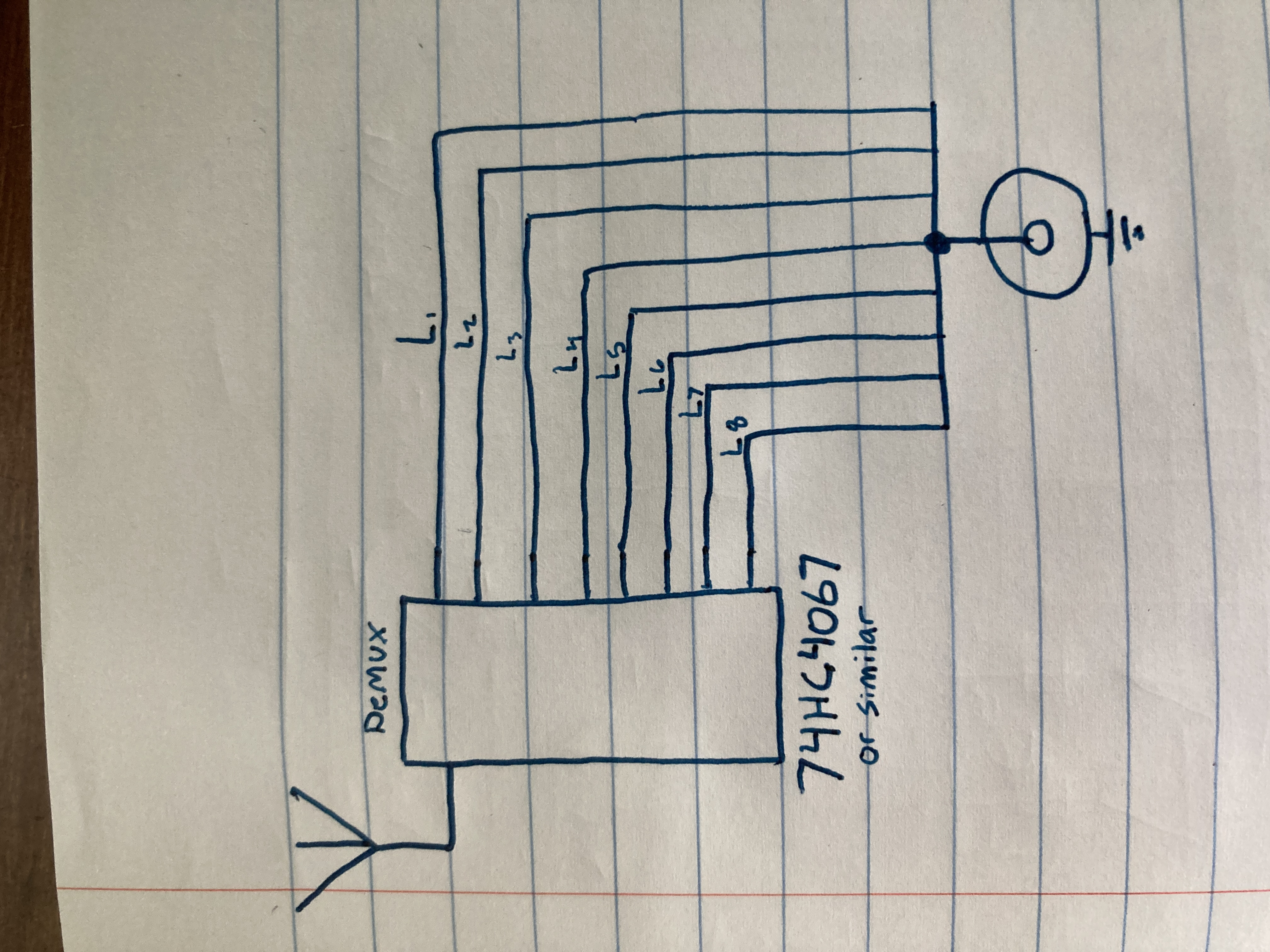
The resolution of this time difference unit is limited by the number of output channels of the DMUX. More output channels means more granularity in the phase shift that can be achieved. Most digitally programmable phase shifting IC's are 6-bit or 8-bit. This means there are 26(64) or 28(256) possible discrete phase shifts, resulting in a phase resolution of 5.6° (360/64), or about 1.4° (360/256), respectively. For a higher resolution time difference unit, the demultiplexer must have a large amount of output channels, probably about 64. I will simply daisy chain multiple 16:1 demultiplexers together to switch between many microstrip lengths, ignoring the marginal insertion loss. The propagation delay of the chained demultiplexer may also present an issue, but if the delay is constant across all channels, I dont foresee any problems. To enable bidirectional operation (both transmit and receive capabilites), there are a couple of options (note that I simplify discussion here by referencing a single MUX IC instead of a system of chained ones): 1. Insert a second demultiplexer at the opposite end of the device. This would create a MUX/DMUX pair that would receive the same control signals. The output of the demultiplexer at the input would route signals through the delay line to the same input of the multiplexer. When signals are travelling in the opposite direction, the roles would be reversed. 2. Use a single bidirectional multiplexer/demultiplexer IC with tri-state logic (low, high, high-impedance). The active channel would present a low resistace for signal to pass through, while the other output buffers would be disconnected from the circuit, presenting a high impedance. When transmitting, the signal (travelling from bottom to top in the picture above), will contact all delay lines. However, since only the selected channel in the demultiplexer chip (acting as a multiplexer in this case) has a path to the antenna, it will travel through this delay line. This method does not require the use of a second system of chained demultiplexers to route signals, so I'll probably go with this one.
The actual lengths of the transmission lines depend on the frequency of operation, the velocity of propagation of the copper strip, and the time difference to be inserted. The phase shift of time delay units are usually measured in multiples of wavelength, not precise phase differences, so the accuracy of construction is critical. The calculation of these lengths will be covered in a future article, along with the design of a demultiplexer with a number of output channels suitable for relatively fine resolution time delays.